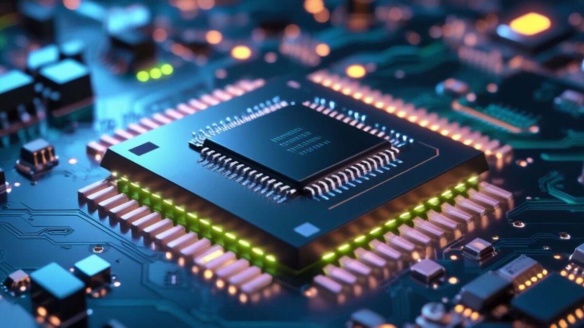
By the end of the year, Taiwan’s top microchip maker, TSMC, intends to begin mass manufacturing next-generation “2-nanometre” chips.
What It Means and Why It Matters
AFP examines what it entails and its significance:
What Are Their Options?
As manufacturers pack more tiny electronic components onto chips, their processing power has grown significantly over the years.
This has led to significant technical advancements in everything from vehicles to smartphones, as well as the introduction of ChatGPT and other artificial intelligence applications.
Modern 2-nanometer (2nm) chips are designed differently to accommodate even more of the essential components known as transistors, and they operate better and consume less energy than earlier models.
According to US computer giant IBM, the new chip technology will help speed up laptops, lower the carbon footprint of data centers, and enable self-driving vehicles to detect things more quickly.
According to Jan Frederik Slijkerman, senior sector strategist at Dutch bank ING, “this helps both consumer gadgets — allowing quicker, more powerful on-device AI — and data center AI processors, which can run huge models more effectively.”
Who Produces Them?
According to Slijkerman, making 2nm chips—the most sophisticated in the industry—requires modern lithography tools, profound understanding of the manufacturing process, and large expenditures and is “very hard and costly” (AFP).
Only a few businesses can accomplish it, including the US company Intel, South Korea’s Samsung, and TSMC, which controls the chip manufacturing sector.
According to TrendForce analyst Joanne Chiao, TSMC is leading, with the other two “still in the stage of boosting yield” and missing large-scale clients.
In order to produce 2nm chips in large quantities by 2027, Japanese chipmaker Rapidus is also constructing a facility in northern Japan.
What Effect Does This Have on Politics?
It has not always been easy for TSMC to produce 2nm in large quantities.
In August, Taiwanese authorities accused three individuals of stealing 2nm chip trade secrets in order to support Tokyo Electron, a Japanese firm that manufactures equipment for TSMC.
“This case includes important national core technology essential to Taiwan’s economic lifeblood,” the office of high prosecutors said at the time.
There are also commercial conflicts and geopolitical issues.
This summer, Nikkei Asia revealed that TSMC, which has customers including Apple and Nvidia, would not employ Chinese chipmaking machinery in its 2nm manufacturing lines in order to prevent interruption from any US regulations.
With “the end of the decade” as their current goal, TSMC claims they want to accelerate 2nm chip manufacture in the US.
What Is the Size of Two Nanometers?
very small—an atom is around 0.1 nanometers wide, for comparison.
However, 2nm is only a marketing phrase and has nothing to do with the actual size of the chip or any of its components.
Rather, Chiao told AFP that “the fewer the number, the greater the density” of these elements.
According to IBM, 2nm designs can fit up to 50 billion transistors—tiny parts smaller than a virus—on a fingernail-sized device.
Silicon slices are etched, processed, and mixed with thin layers of other materials to make the transistors.
A smaller chip or one of the same size with more processing power is the outcome of a greater transistor density.
Are Chips Going to Get Any Better?
Indeed, TSMC is already working on “1.4-nanometre” technology, which is expected to enter full production in 2028, with Samsung and Intel following closely after.
According to Taiwanese media, TSMC began high-volume 3nm manufacture in 2023 and is now constructing a 1.4nm chip facility in Taichung.
Japan’s Rapidus claims that 2nm chips are “perfect for AI servers” and will “form the cornerstone of the next-generation digital infrastructure” in spite of the significant expenses and technical difficulties associated with them.